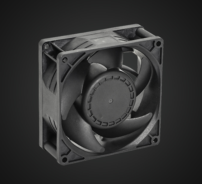
DZ09238-F04

类 型:双滚珠
风 量:90.57~123.50CFM
尺 寸:80x80x38mm
额定电压:12V
重 量:153.0g
DZ08038-F06
类 型:双滚珠
风 量:90.57~123.50CFM
尺 寸:80x80x38mm
额定电压:12V
重 量:153.0g
DZ12038-F05
类 型:双滚珠
风 量:90.57~123.50CFM
尺 寸:80x80x38mm
额定电压:12V
重 量:153.0g
DA04056-F01
类 型:双滚珠
风 量:90.57~123.50CFM
尺 寸:80x80x38mm
额定电压:12V
重 量:153.0g


Basic knowledge of electronic components - semiconductor devices
2022-06-14 14:39:58
Click:
“
China's semiconductor device model naming method The semiconductor device model consists of five parts (field effect devices, semiconductor special devices, composite tubes, PIN tubes, and laser devic
”
1. China's semiconductor device model naming method The semiconductor device model consists of five parts (field effect devices, semiconductor special devices, composite tubes, PIN tubes, and laser devices have only the third, fourth, and fifth parts). The meanings of the five parts are as follows: Part 1: Use numbers to represent the number of effective electrodes of the semiconductor device. 2-diode, 3-transistor Part 2: The material and polarity of semiconductor devices are represented by Chinese pinyin letters. When representing diodes: A-N type germanium material, B-P type germanium material, C-N type silicon material, D-P type silicon material. When representing triode: A-PNP type germanium material, B-NPN type germanium material, C-PNP type silicon material, D-NPN type silicon material. The third part: The inner type of semiconductor device is represented by Chinese pinyin letters. P-common tube, V-microwave tube, W-voltage regulator, C-parameter tube, Z-rectifier tube, L-rectifier stack, S-tunnel tube, N-damping tube, U-photoelectric device, K-switch tube , X-low frequency small power tube (F<3MHz, Pc<1w), g-high="" frequency="" small="" power="" tube="" f="">3MHz, Pc<1W), D-low frequency high power tube (f<3mhz, pc="">1W), A-high frequency high power tube (f>3MHz, Pc>1W), T-semiconductor thyristor (controlled rectifier), Y-body effect device, B-avalanche tube, J-step recovery tube, CS-field effect tube , BT-semiconductor special device, FH-composite tube, PIN-PIN tube, JG-laser device. The fourth part: the serial number is represented by numbers. The fifth part: the specification number is represented by the Chinese pinyin letters. For example: 3DG18 represents the NPN type silicon material high-frequency triode II. The model naming method of Japanese semiconductor discrete devices The semiconductor discrete devices produced in Japan are from five to seven. part composition. Usually only the first five parts are used, and the meanings of the symbols of each part are as follows: Part 1: Use numbers to indicate the number or type of effective electrodes of the device. 0 - Photoelectric (ie photosensitive) diode triode and the combination of the above devices, 1 - Diode, 2 Triode or other devices with two pn junctions, 3 - Other devices with four active electrodes or three pn junctions, .....and so on. Part II: JEIA registration mark of Japan Electronics Industry Association. S- represents a semiconductor discrete device registered with the Japan Electronics Industry Association JEIA. Part 3: Use letters to indicate the polarity and type of materials used in the device. A-PNP type high frequency tube, B-PNP type low frequency tube, C-NPN type high frequency tube, D-NPN type low frequency tube, F-P gate thyristor, G-N gate thyristor, H-N base unijunction transistor , J-P channel field effect transistor, K-N channel field effect transistor, M-triac. Part 4: Use numbers to indicate the serial number registered with the Japan Electronics Industry Association JEIA. An integer with more than two digits - starting from "11", it indicates the serial number registered with the Japan Electronics Industry Association JEIA; devices with the same performance from different companies can use the same serial number; the larger the number, the more recent products. Part 5: Use letters to represent the improved product marks of the same model. A, B, C, D, E, F indicate that this device is an improved product of the original model. 3. Nomenclature of American semiconductor discrete device models The nomenclature of American transistors or other semiconductor devices is confusing. The naming method of semiconductor discrete devices of the American Electronics Industry Association is as follows: Part 1: The type of device use is represented by a symbol. JAN-military grade, JANTX-special military grade, JANTXV-super special military grade, JANS-astronautic grade, (none)-non-military supplies. Part II: Use numbers to represent the number of pn junctions. 1-diode, 2=triode, 3-three pn junction devices, n-n pn junction devices. Part III: Electronic Industries Association (EIA) registered mark. N - This device is registered with the Electronic Industries Association (EIA). The fourth part: the registration sequence number of the American Electronics Industry Association. Multi-Digit - The device's serial number registered with the Electronic Industries Association. Part 5: Use letters to indicate device binning. A, B, C, D, .....-different grades of the same type of device. Such as: JAN2N3251A represents PNP silicon high-frequency low-power switching transistor, JAN-military grade, 2-transistor, N-EIA registration mark, 3251-EIA registration sequence number, A-2N3251A file. 4. Model naming method of semiconductor devices of the International Federation of Electronics Industry Germany, France, Italy, the Netherlands, Belgium and other European countries and Eastern European countries such as Hungary, Romania, Yugoslavia, Poland, etc., mostly adopt the model naming method of semiconductor discrete devices of the International Federation of Electronics Industry. This nomenclature consists of four basic parts, and the symbols and meanings of each part are as follows: Part 1: Use letters to indicate the materials used in the device. A- The forbidden band width of the material used in the device is Eg=0.6~1.0eV, such as germanium, B- the material used in the device is Eg=1.0~1.3eV, such as silicon, C- The material used in the device is Eg>1.3eV, such as gallium arsenide, D- Eg<0.6eV of materials used in devices, such as indium antimonide, composite materials used in E-devices, and materials used in photovoltaic cells Part II: Types and main features of devices are represented by letters. A-detection switch mixing diode, B-varactor diode, C-low frequency low-power transistor, D-low frequency high-power transistor, E-tunnel diode, F-high-frequency low-power transistor, G-composite devices and other devices, H -Magnetic diode, K-Hall element in open magnetic circuit, L-High frequency high-power triode, M-Hall element in closed magnetic circuit, P-Photosensitive device, Q-Light-emitting device, R-Low power thyristor , S-low-power switch tube, T-high-power thyristor, U-high-power switch tube, X-multiplier diode, Y-rectifier diode, Z-zener diode. Part 3: Use numbers or letters plus numbers to indicate the registration number. Three digits - representing the registration serial number of general-purpose semiconductor devices, one letter plus two digits - representing the registration serial number of special-purpose semiconductor devices. Part 4: Binning of devices of the same type by letter. A, B, C, D, E .....-a sign that the devices of the same model are classified according to a certain parameter.
In addition to the four basic parts, suffixes are sometimes added to distinguish characteristics or to further classify. Common suffixes are as follows: 1. The suffix of the Zener diode model. The first part of the suffix is a letter, indicating the allowable error range of the stable voltage value, the letters A, B, C, D, E indicate that the allowable error is ±1%, ±2%, ±5%, ±10%, ± 15%; the second part of the suffix is a number, which represents the integer value of the nominal stable voltage; the third part of the suffix is the letter V, which represents the decimal point, and the number after the letter V is the decimal value of the nominal stable voltage of the Zener tube. 2. Suffix of rectifier diode: The suffix of rectifier diode is a number, which indicates the maximum reverse peak withstand voltage value of the device, and the unit is volts. 3. The suffix of the thyristor model: the suffix of the thyristor model is also a number, which is usually marked with the smaller value of the maximum reverse peak withstand voltage value and the maximum reverse turn-off voltage. Such as: BDX51- represents NPN silicon low-frequency high-power transistor, AF239S- represents PNP germanium high-frequency low-power transistor.


TEL
+86-769-21 665206

JENNIE@MERRYELC.COM

WEB
WWW.MERRYELC.COM

Dongguan Merry Electronic CO.,LTD
Dongguan Merry Electronic CO., LTD Was established in year of 2013,Mainly engaged in design, development and sales semiconductors...

点击右上角
分享给朋友吧
Copyright ©2022 Dongguan Merry Electronic CO.,LTD All Rights Reserved